|
1Page

SD686X
CURRENT MODE PWM+PFM CONTROLLER WITH BUILT-IN HIGH VOLTAGE
MOSFET
DESCRIPTION
SD686X is current mode PWM+PFM controller with built-in high-
voltage MOSFET used for SWPS, with low standby power and low
start current for power switch. In standby mode, the circuit enters
burst mode to reduce the standby power dissipation. The switch
frequency is 25~67KHz with jitter frequency for low EMI.
Built-in peak current compensation circuit makes the limit output
power stable even with different input AC voltage. Limit output
power can be adjusted through the resistor. Maximum peak current
compensation during power-on reduces pressure on transformer to
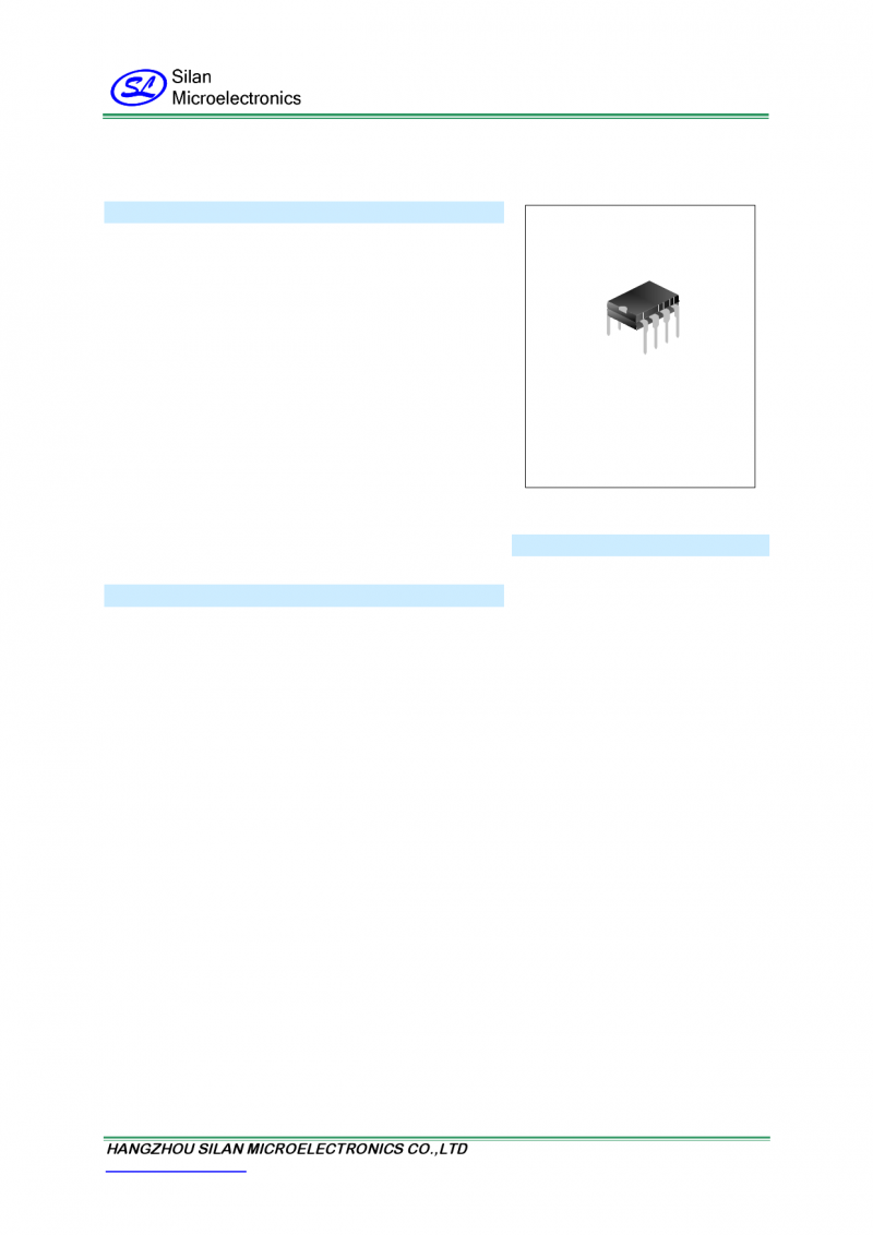
DIP-8-300-2.54
avoid saturation, the peak current compensation will decrease for
balance after power-on.
It integrates various protections such as undervoltage lockout,
overvoltage protection, overload protection, lead edge blanking,
primary winding overcurrent protection and thermal shutdown. The
circuit will restart until normal if protection occurs.
APPLICATIONS
FEATURES
* SWPS
* Energy Star 2.0 standard
* Lower start-up current (3µA)
* Various switching frequency following load for the higher
efficiency
* Frequency jitter for low EMI
* Overvoltage, overcurrent, overload and over temperature
protections.
* Adjustable limit output power
* Undervoltage lockout
* Built-in high voltage MOSFET
* Auto restart mode
* Peak current compensation
* Maximum peak current compensation for initialization
* Burst mode
* Cycle by cycle current limit
HANGZHOU SILAN MICROELECTRONICS CO.,LTD
Http://www.silan.com.cn
REV:1.0
2010.03.12
Page 1 of 10


SD686X
ORDERING INFORMATION
Part No.
SD6860
SD6861
SD6862
SD6863
SD6864
Package
DIP-8-300-2.54
Marking
SD6860
SD6861
SD6862
SD6863
SD6864
TYPICAL OUPUT POWER CAPABILITY
Part No.
SD6860P65K67
SD6861P65K67
SD6862P65K67
SD6863P65K67
SD6864P65K67
190~265V
Adapter
Open
7W 9W
10W
14W
12W
17W
14W
19W
16W
21W
BLOCK DIAGRAM
Material
Pb free
Pb free
Pb free
Pb free
Pb free
Package Type
Tube
Tube
Tube
Tube
Tube
85~265V
Adapter
5W
8W
10W
12W
14W
Open
7.2W
12W
14W
15W
18W
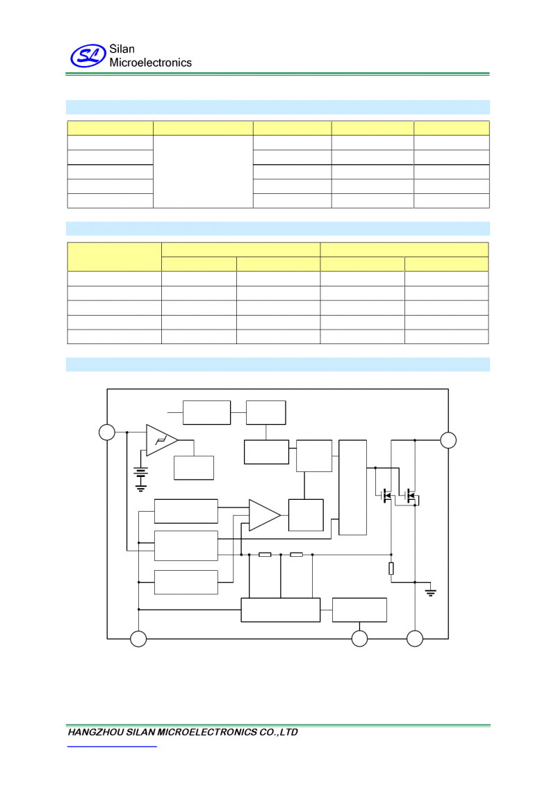
VCC
FB Reduced
frequency
control
14.8V
7.6V
Internal
Bias
Level shift
Over voltage, over
current, over load and
over temperature
protections
Burst mode
control
FB
OSC
Frequency S
jitter Q
R
COMP
Leading
Edge
Blanking
Control
Driver
Peak current
compensation
Limit output
power adjust
ADJ
DR
GND
HANGZHOU SILAN MICROELECTRONICS CO.,LTD
Http://www.silan.com.cn
REV:1.0
2010.03.12
Page 2 of 10

SD686X
ABSOLUTE MAXIMUM RATING
Characteristics
Symbol
Drain-Gate Voltage (RGS=1MΩ)
VDGR
Gate-Source (GND) Voltage
VGS
SD6860
Drain Current Pulse
note1
SD6861
SD6862
SD6863
IDM
SD6864
SD6860
Continuous Drain SD6861
Current
(Tamb=25°C)
SD6862
SD6863
ID
SD6864
SD6860
Signal Pulse
SD6861
Avalanche
Energynote2
SD6862
SD6863
EAS
SD6864
Power Supply Voltage
VCC,MAX
Feedback input voltage
VFB
Limit output power voltage
VADJ
Total Power Dissipation
PD
Darting
Operating Junction Temperature
TJ
Operating Temperature
Tamb
Storage Temperature
TSTG
Note: 1. Pulse width is limited by maximum junction temperature;
2. L=51mH, TJ=25°C(start)。
Rating
650
±30
4
6
8
11
14
1
1.5
2
3
4
15
30
68
140
200
28
-0.3~8
-0.3~8
1.5
0.017
+170
-25~+85
-55~+150
Unit
V
V
A
A
mJ
V
V
V
W
W/°C
°C
°C
°C
ELECTRICAL CHARACTERISTICS (for MOSFET, unless otherwise specified, Tamb=25°C)
Characteristics
Drain-Source Breakdown Voltage
Zero Gate Voltage Drain Current
Static Drain-Source
On Resistance
SD6860
SD6861
SD6862
SD6863
SD6864
Symbol
Test conditions
BVDSS VGS=0V, ID=50µA
VDS=650V, VGS=0V
IDSS VDS=480V, VGS=0V
Tamb=125°C
RDS(ON) VGS=10V, ID=0.5A
Min.
650
—
Typ.
—
—
— —
— 14.0
— 8.0
— 5.0
— 4.0
— 3.0
Max.
—
50
Unit
V
µA
200 µA
16.8
9.6
6.0 Ω
4.8
3.6
HANGZHOU SILAN MICROELECTRONICS CO.,LTD
Http://www.silan.com.cn
REV:1.0
2010.03.12
Page 3 of 10
|


