Даташит mc34119 pdf ( datasheet )

Datasheet Download — Unisonic Technologies

Номер произв MC34119
Описание LOW POWER AUDIO AMPLIFIER
Производители Unisonic Technologies
логотип  

1Page

No Preview Available !

UNISONIC TECHNOLOGIES CO., LTD
MC34119
LINEAR INTEGRATED CIRCUIT
LOW POWER AUDIO
AMPLIFIER

DESCRIPTION

The UTC MC34119 is a low power audio amplifier IC intended for
the telephone applications, such as in speakerphones. It provides
differential speaker outputs to maximize output swing at low supply
voltages. Coupling capacitor to the speaker is not required. Open
loop gain is 80dB, and the closed loop gain is set with two external
resistors. The Mute pin permits powering down and/or muting the
input signal.
SOP-8
DIP-8

FEATURES

*Wide operating supply voltage: VCC=2V~16V

*Low quiescent supply current (ICC=2.7mA, typ)

*Medium output power (POUT=250mW at VCC=6V,

RL=32ohm, THD=10%)

*Load impedance range (8 to 100ohm)
*Low distortion

*Mute function (ICC=65μA, typ)

*Minimum number of external parts required
www.DataSheet4U.com
TSSOP-8
*Pb-free plating product number:MC34119L

ORDERING INFORMATION

Ordering Number
Normal
Lead Free Plating
MC34119-D08-T
MC34119L-D08-T
MC34119-P08-R
MC34119L-P08-R
MC34119-P08-T
MC34119L-P08-T
MC34119-S08-R
MC34119L-S08-R
MC34119-S08-T
MC34119L-S08-T
Package
DIP-8
TSSOP-8
TSSOP-8
SOP-8
SOP-8
Packing
Tube
Tape Reel
Tube
Tape Reel
Tube
www.unisonic.com.tw
Copyright 2005 Unisonic Technologies Co., Ltd
1 of 8
QW-R107-038,E

No Preview Available !

MC34119

PIN CONFIGURATION

MUTE 1
RR 2

IN + 3

IN 4
LINEAR INTEGRATED CIRCUIT
8 OUT2
7 GND

6 VCC

5 OUT1
PIN NAME
DESCRIPTION
This pin can be used to power down the IC to converse power, or for muting, or
1
Mute
both. When at a logic “LOW” (less than 0.8V), the IC is enabled for normal
operation. When at a logic “HIGH” (2V to Vcc), the IC is disabled. If Mute is open,
that is equivalent to a logic “LOW”.

2 Ripple A capacitor at this pin increase power supply rejection, and affects turn-on time.

Rejection This pin can be left open if the capacitor at pin 3 is sufficient.

Analog Ground for the amplifiers. A 1μF capacitor at this pin ( with a 5μF

3 Input(+) capacitor at pin 2) provides 52dB( typ) of power supply rejection. Turn-on time of

the circuit is affected by the capacitor on this pin. This pin can be used as an
alternative input.
Amplifier input. The input capacitor and resistor set low frequency roll-off and
4 Input(-) input impedance. The feedback resistor is connected between this pin and output
1.
5 Output 1 Amplifier output 1. The DC level is about (Vcc~0.7V)/2.
6 Vcc DC supply voltage is applied to this pin(Vcc=2~16V).
7 GND Ground pin.

8 Output 2 Amplifier output 2. This signal is equal in amplitude, but 180°out of phase with

that output 1, the DC level is about (Vcc~0.7V)/2.
UNISONIC TECHNOLOGIES CO., LTD
www.unisonic.com.tw
2 of 8
QW-R107-038,E

No Preview Available !

MC34119

BLOCK DIAGRAM

IN +

IN
Amp 1
LINEAR INTEGRATED CIRCUIT
OUT1

Vcc Bias

RR
GND
OUT2
MUTE
UNISONIC TECHNOLOGIES CO., LTD
www.unisonic.com.tw
3 of 8
QW-R107-038,E

Всего страниц 8 Pages
Скачать PDF

MC34119 Datasheet PDF — Motorola Semiconductors

Part Number MC34119
Description LOW POWER AUDIO AMPLIFIER
Manufacturers Motorola Semiconductors 
Logo  

There is a preview and MC34119 download ( pdf file ) link at the bottom of this page.

Total ( 12 pages )

Preview 1 page

No Preview Available !

Order this document by MC34119/D
Low Power Audio Amplifier
The MC34119 is a low power audio amplifier intergrated circuit intended
(primarily) for telephone applications, such as in speakerphones. It provides
differential speaker outputs to maximize output swing at low supply voltages
(2.0 V minimum). Coupling capacitors to the speaker are not required. Open
loop gain is 80 dB, and the closed loop gain is set with two external resistors.
A Chip Disable pin permits powering down and/or muting the input signal.
The MC34119 is available in standard 8–pin DIP, SOIC package, and
TSSOP package.

• Wide Operating Supply Voltage Range (2.0 V to 16 V), Allows

Telephone
Line Powered Applications

• Low Quiescent Supply Current (2.7 mA Typ) for Battery

Powered Applications

• Chip Disable Input to Power Down the IC

• Low Power–Down Quiescent Current (65 µA Typ)

• Drives a Wide Range of Speaker Loads (8.0 Ω and Up)

• Output Power Exceeds 250 mW with 32 Ω Speaker

• Low Total Harmonic Distortion (0.5% Typ)

• Gain Adjustable from <0 dB to >46 dB for Voice Band

• Requires Few External Components

MAXIMUM RATINGS
Rating
Supply Voltage
Maximum Output Current at VO1, VO2
Maximum Voltage @ Vin, FC1, FC2, CD
Applied Output Voltage to VO1, VO2 when disabled
Junction Temperature

NOTE: ESD data available upon request.

Value
–1.0 to +18

±250

–1.0, VCC + 1.0
–1.0, VCC + 1.0
–55, +140
Unit
Vdc
mA
Vdc

°C

MC34119
LOW POWER
AUDIO AMPLIFIER
SEMICONDUCTOR
TECHNICAL DATA
8
1
P SUFFIX
PLASTIC PACKAGE
CASE 626
8
1
D SUFFIX
PLASTIC PACKAGE
CASE 751
(SO–8)
8
1
DTB SUFFIX
PLASTIC PACKAGE
CASE 948J
(TSSOP)
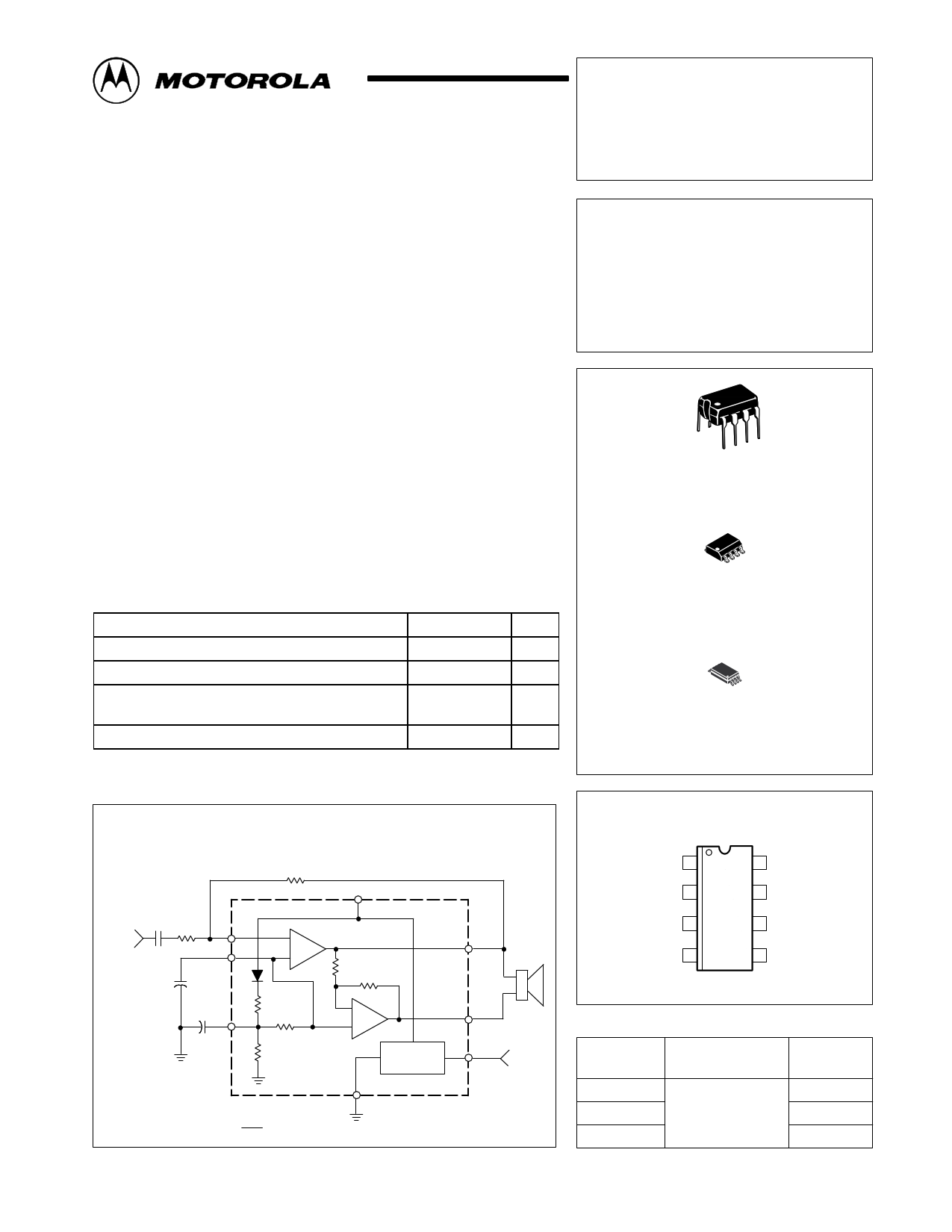
Block Diagram and Simplified Application
Rf
75 k
6 VCC
Audio
Input
Ci
0.1
Ri
3.0 k
Vin
FC1
C1

1.0 µF

C2*

5.0 µF

FC2
* = Optional
Differential Gian = 2 x
4

3 + #1

4.0 k
4.0 k
5 VO1
Speaker
50 k

2 125 k


#2
+

8 VO2

50 k Bias 1 CD Chip

Circuit
Disable
MC34119
7
Gnd
Rf
Ri This device contains 45 active transistors.
MOTOROLA ANALOG IC DEVICE DATA
PIN CONNECTIONS
CD 1
FC2 2
8 VO2
7 Gnd
FC1 3
6 VCC
Vin 4
5 VO1
(Top View)
ORDERING INFORMATION
Device
Operating
Temperature Range Package
MC34119P

MC34119D TA = –20° to +70°C

MC34119DTB
Plastic DIP
SO–8
TSSOP

Motorola, Inc. 1996

Rev 1
1

MC34119
of each of the three curves is defined by the power level at
which 10% distortion occurs. The center flat portion of each
curve is defined by the maximum output current capability of
the MC34119. The right (descending) portion of each curve is
defined by the maximum internal power dissipation of the IC

at 25°C. At higher ambient temperatures, the maximum load

power must be reduced according to the above equations.
Operating the device beyond the current and junction
temperature limits will degrade long term reliability.
Layout Considerations
Normally a snubber is not needed at the output of the
MC34119, unlike many other audio amplifiers. However, the
PC board layout, stray capacitances, and the manner in
which the speaker wires are configured, may dictate
otherwise. Generally, the speaker wires should be twisted
tightly, and not more than a few inches in length.
Figure 2. Amplifier #1 Open Loop Gain and Phase
100 0
36
80
Phase
72
108
60 144
Gain
40
180
20

100 1.0 k
10 k
100 k
1.0 M
f, FREQUENCY (Hz)
Figure 3. Differential Gain versus Frequency
36
Rf = 150 k, Ri = 6.0 k
32
24
16
8

100
Rf = 75 k, Ri = 3.0 k
Rf
0.1
Input
Ri –+#1
VO1
VO2 VO
#2
1.0 k 10 k 20 k
f, FREQUENCY (Hz)
MOTOROLA ANALOG IC DEVICE DATA
5


Preview 5 Page
Information Total 12 Pages
Link URL
Download

Share Link :

Electronic Components Distributor

SparkFun Electronics Allied Electronics DigiKey Electronics Arrow Electronics

Mouser Electronics Adafruit Element14 Chip One Stop

Featured Datasheets

Part Number Description Manufacturers
MC3411 The function is P-Channel 20-V (D-S) MOSFET. Freescale
MC34114 The function is TELEPHONE SPEECH NETWORK WITH DIALER INTERFACE. Motorola Semiconductors
MC34115 The function is CONTINUOUSLY VARIABLE SLOPE DELTA MODULATOR/DEMODULATOR. Motorola Semiconductors

Quick jump to:

MC34 
1N4 
2N2 
2SA 
2SC 
74H 
ADC 
BC 
BF 
BU 
CXA 
HCF 
IRF 
KA 
KIA 
LA 
LM 
MC 
NE 
ST 
STK 
TDA 
TL 
UA